| |
|
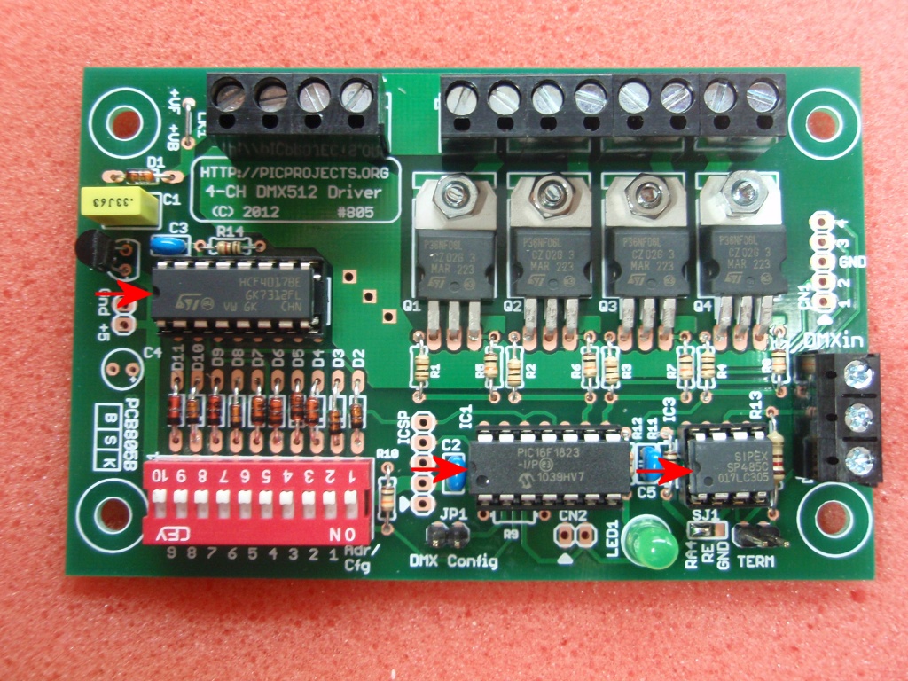
4
Channel DMX512 Driver
for PIC16F1823
|
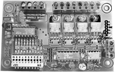 |
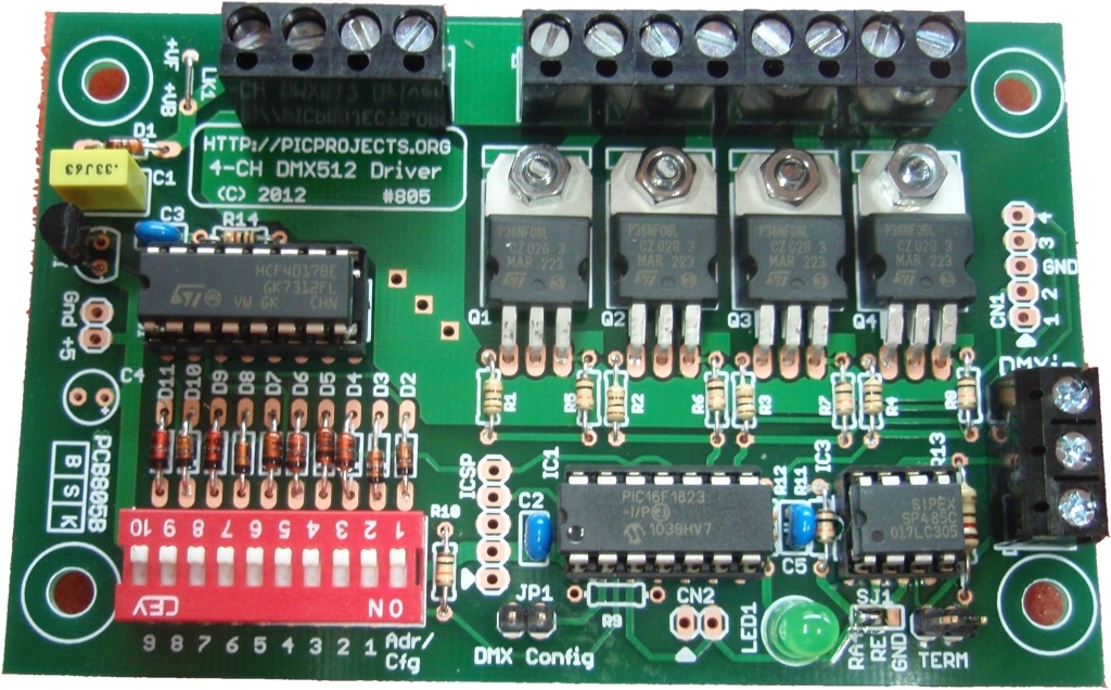
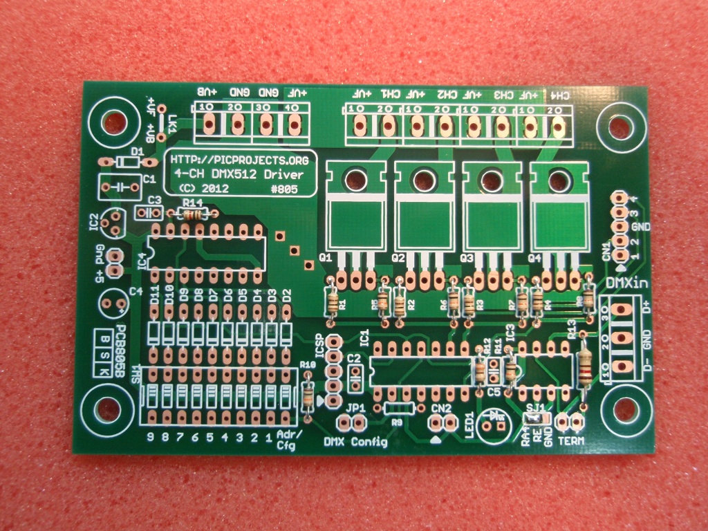
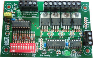
4-channel DMX512 PWM LED
Driver Board
 |
-
The original
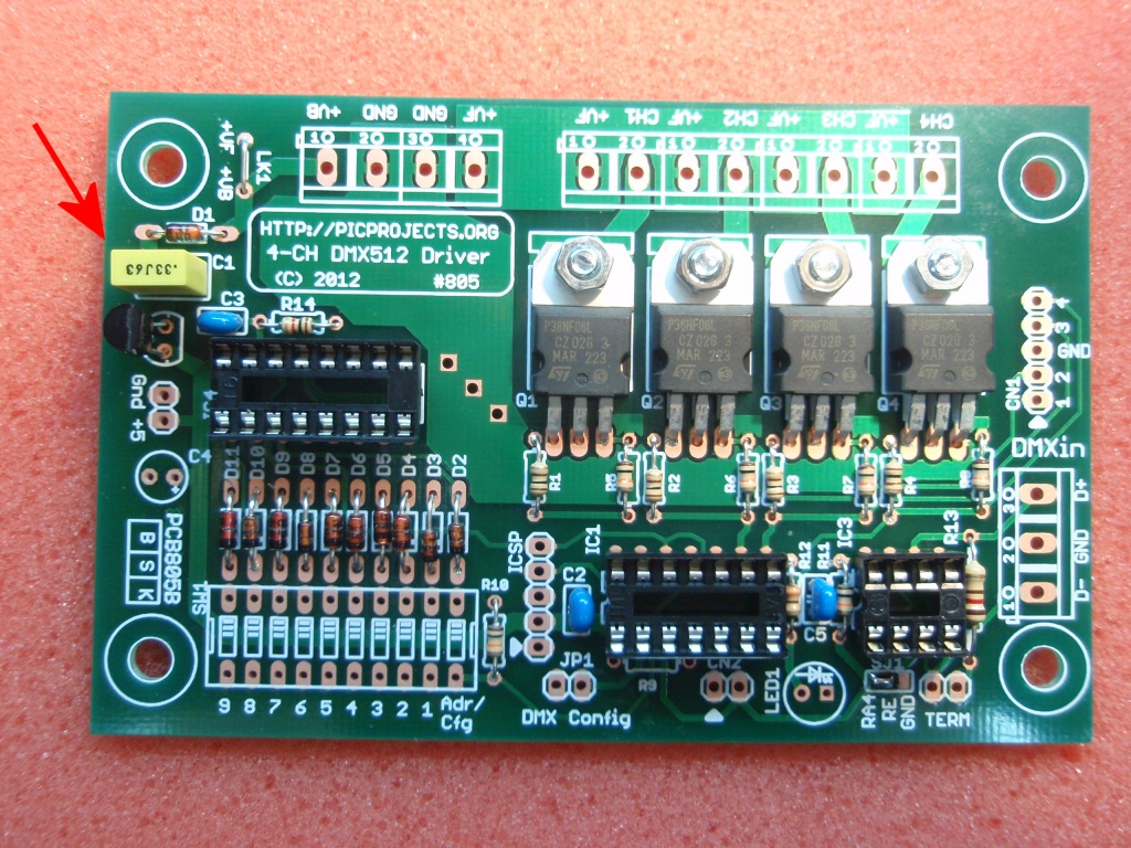
DMX512 driver project #800 is now redesigned to incorporate the optional address configuration switch on the main PCB.
-
The
no-switches in-band DMX configuration feature is still
retained
-
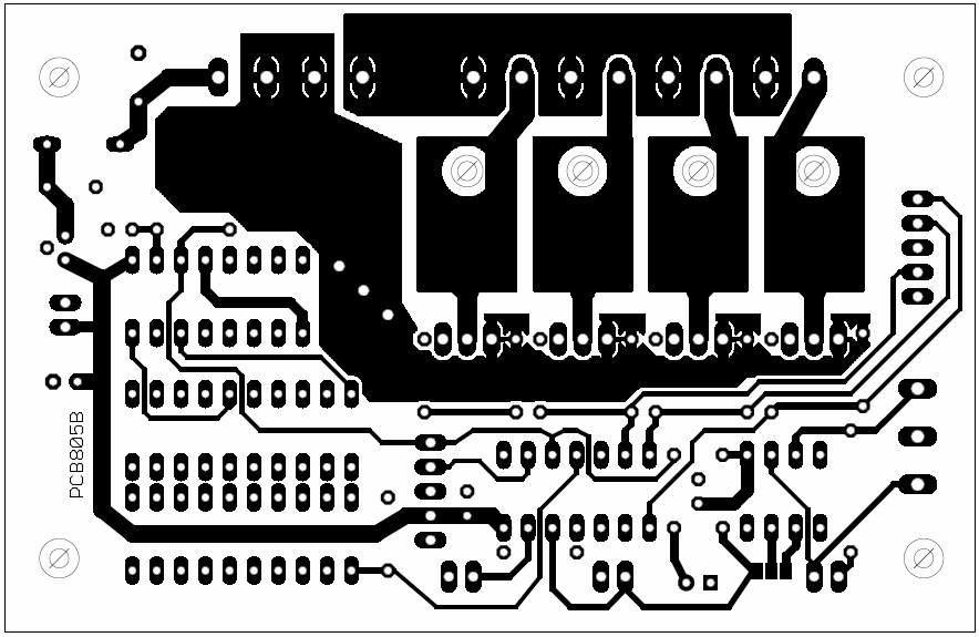
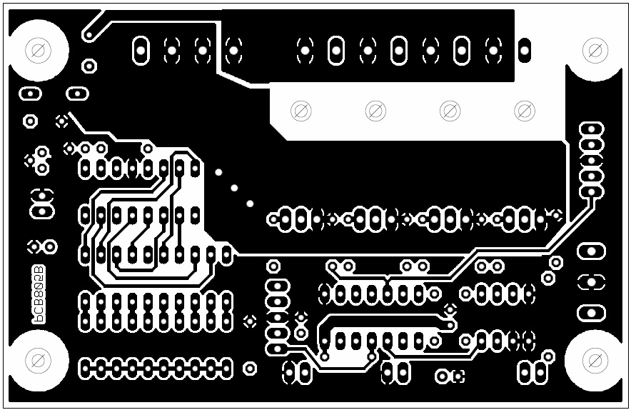
Double sided PCB has resulted in a more compact
board size.
-
Firmware has
been updated to run a latest generation
enhanced midrange PIC16F1823 processor.
|
Description
This project is a 4 channel
DMX512 driver board. It features four power MOSFETs that
can be configured to operate in PWM mode or as on/off outputs.
The driver can be configured to use any four consecutive
addresses across the full 512 channel address range. It can drive LED arrays or low voltage lamps with either an 8
bit (256 step) PWM dimming signal or digital on/off mode under
DMX control.
Feature list:
In keeping with the original
4-channel DMX driver project #800, the firmware supports a
minimal external hardware design.
Although the new PCB805B has a
configuration DIP switch on the board, the DMX base address and
configuration modes are stored in the microcontrollers internal
non-volatile EEPROM. Once settings have been made the
firmware uses the saved settings from the EEPROM if no DIP
switch is detected.
Additionally the original
configuration via in-band DMX channel data is still supported.
Fitting a single jumper puts the firmware into 'in-band' configuration mode. DMX
data sent in the first four channels is saved to the EEPROM
allowing the DMX base address and configuration word to be setup
without the use of the external DIP switch.
Download PDF
manual

The project page for the
previous version of the 4-Channel DMX driver can be found here:
Previous
4-Channel DMX driver
The following options for
the DMX512 PWM Driver are available to buy from
the
Picprojects eShop
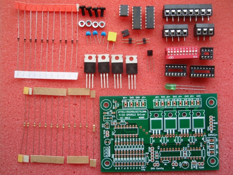
- Complete kit of parts,
including PCB and pre-programmed PIC microcontroller, order
code #805K
- PCB805 only, order code
#805P
- PIC microcontroller
pre-programmed with DMX firmware, order code #PRG805
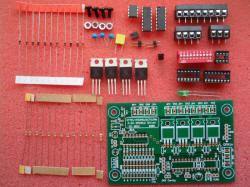
Component List
 |
I no longer have
kits or the PCB805 for this project.
|
|
Component |
Description |
|
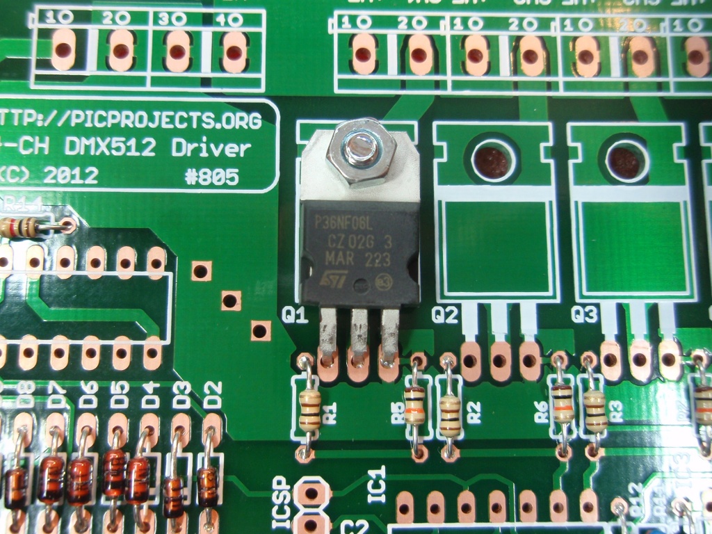
R1,R2,R3,R4 |
120R 0.125 watt
|
|
R5,R6,R7,R8,R10,R11 |
10K 0.125 watt |
| R12 |
330R 0.125 watt |
| R13 |
120R ( 0.25w or
0.5 watt) |
| R14 |
1K0 0.125 watt |
| R9 |
not used |
All
resistors are 5% carbon film.
Where 0.125 (1/8) watt parts are specified these are required
to fit on the PCB due to size constraints. |
| |
|
| C1 |
330nF polyester (5mm
pitch) (or 470nF) |
| C2,C3,C5 |
100nF multilayer
ceramic (2.5mm pitch) |
| C4 |
not used |
| |
|
| D1-D11 |
1N4148 diode |
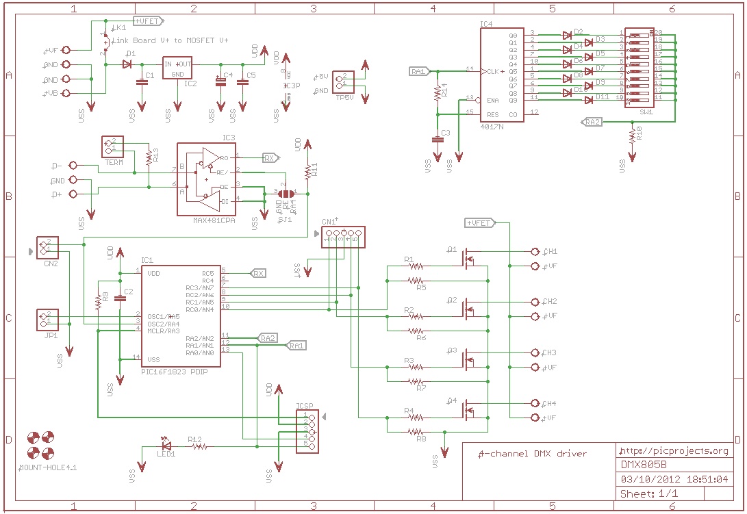
| IC1 |
PIC16F1823-I/P
(Must be programmed with DMX firmware) |
| IC2 |
78L05 voltage
regulator |
| IC3 |
MAX481 (or equivalent
RS485 transceiver) |
| IC4 |
HCF4017B |
|
Q1,Q2,Q3,Q4 |
STP20NF06L logic level
N-MOSFET (STP36NF06L alternate part) |
| LED1 |
5mm LED green |
| |
|
| SW1 |
10-way DIP switch |
| CN1 |
5-pin 0.1" header (not
used) |
| ICSP |
5-pin 0.1" header (not
used) |
| CN2 |
2-pin 0.1" header (not
used) |
| JP1 |
2-pin 0.1" header |
| TERM |
2-pin 0.1" header |
| |
2,54mm jumper links
for shorting JP1 / TERM header |
| |
|
| DMXin |
3-way, 5mm,
screw-terminal |
| Power-in
terminal block |
4-way, 5mm,
screw-terminal, 16 amp (2 x 2-way end stackable) |
| Channel
output terminal block |
8-way, 5mm,
screw-terminal, 16 amp (4 x 2-way end stackable) |
| |
|
| IC1 socket |
14-pin DIP socket |
| IC3 socket |
8-pin DIP socket |
| IC4 socket |
16-pin DIP socket |
|
Miscellaneous item x 4 |
M3 nut + M3 x 6mm
machine screw (to mount MOSFET to PCB) |
Notes:
- Apart from resistor R13
all other resistors are 0.125 (1/8) watt parts. These
are specified for physical space constraint reasons on the
PCB.
- The output driver MOSFETs Q1-Q4 are STP36NF06L or
STP20NF06L. These
are logic level devices designed to operate with a low gate
drive voltage. If an alternative non-logic level part is
substituted you may need to derate the maximum output
current per channel.
- Alternative pin-compatible
parts exist for the RS-485 transceiver, IC3.
- SP485 (EXAR)
- ST485 (ST)
- MAX483 (Maxim)
- MAX485 (Maxim)
- other parts are also available
- The
PIC16F1823-I/P (IC1)
requires programming with the DMX firmware.
Construction notes:
- Please read through
this section at least once before starting assembly of the
PCB
- Assembly is
straightforward. You will need previous experience
soldering electronic components, a suitable soldering iron,
hand tools and a multi-meter.
- All photographs in the
section link to a hi-res 1024x768 image for more detail.
- Refer to the
schematic diagram
and component listing above for component values used in this
project
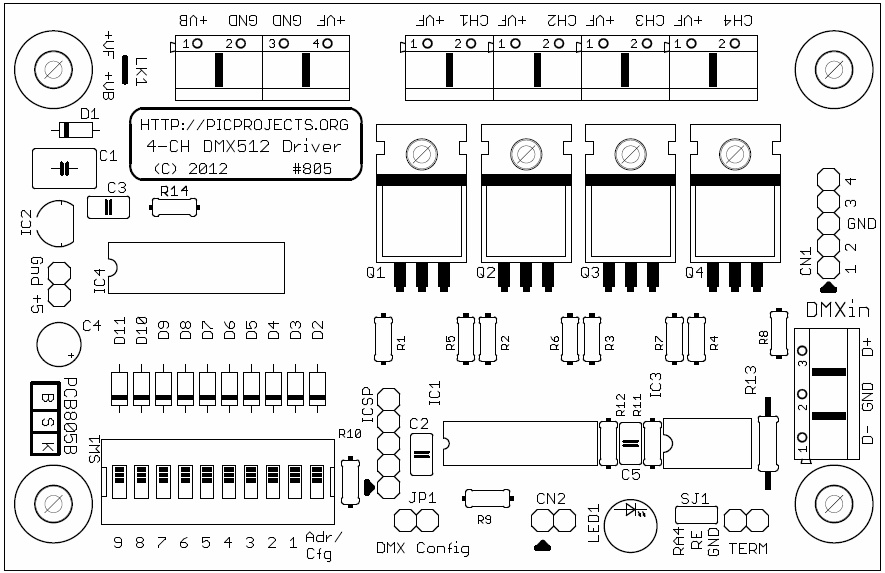
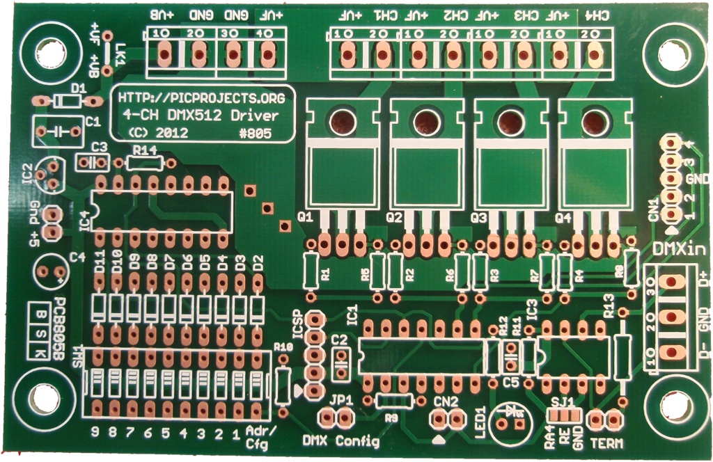
|

Fig.1 |
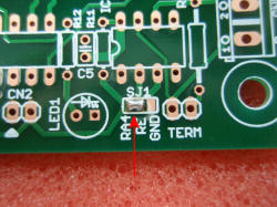
Fig .2 |

Fig. 3 |
Fig 1.
Make sure you assemble the board in an anti-static work
area and follow ESD handling precautions, particularly
when installing the four MOSFET devices (Q1,2,3,4)
- The MOSFETs are
packed in a separate anti-static bag - don't remove
them until needed.
- IC's 1,3 & 4 are
shipped on black anti-static foam - don't remove
them until needed.
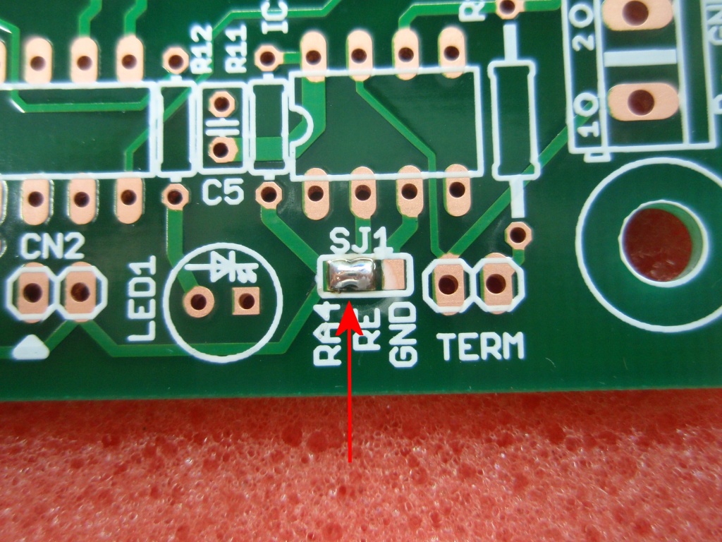
Fig 2. Start by
placing a blob of solder across the RA4-RE pads of SJ1
solder jumper as shown.
 Do not allow solder between the RE and GND pads.
Fig 3. Solder
all the resistors in place. It doesn't matter
which way round they go, the colour bands only indicate
the resistance value. It is important that the
correct value resistors are placed in the correct
locations.
The 0.125 watt resistor
are quite small and the coloured bands are not easy to
read. Be sure to identify them correctly (if in
doubt use
a Multimeter on the resistance range setting to check
the value)
 120R [brown - red - brown
- gold ] R1,R2,R3,R4,
120R [brown - red - brown
- gold ] R1,R2,R3,R4,
120R [brown - red - brown - gold ] R13 (R13 is the larger
0.25 watt resistor)
 330R [orange - orange - brown - gold ] R12
 1K0 [brown - black
-red - gold ] R14
1K0 [brown - black
-red - gold ] R14
 10K [brown - black -orange
- gold ] R5,R6,R7,R8,R10,R11
10K [brown - black -orange
- gold ] R5,R6,R7,R8,R10,R11
Resistor position R9 is not used with this project.
|

Fig.4 |

Fig.5 |

Fig.6 |
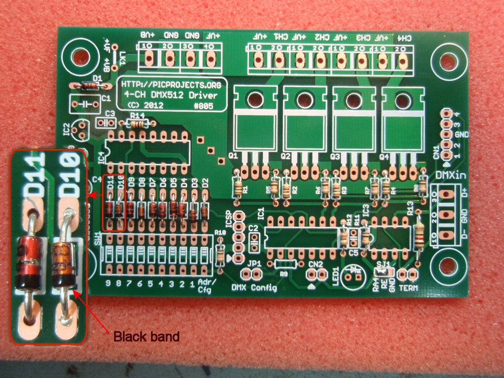
| Fig 4.
Fit the diodes D1 to D11. These are all the same
1N4148 type.
Each diode has a black band on one end of the body.
Fit all the diodes so the black band on the diode
corresponds to the white band on the component screen
print overlay. Refer to the photo in Fig 4.
Fig 5. Install
the three 100nF capacitors to positions C2,C3 and C5.
These are marked '104' on the body.
Fig 6. Install
the four MOSFETs Q1,Q2,Q3,Q4
 MOSFETs are static sensitive devices. Avoid
touching the pins and handle by the main body only.
MOSFETs are static sensitive devices. Avoid
touching the pins and handle by the main body only.
Install the MOSFETs one
at a time.
- Place the pins
through the PCB and then push down on the body of the MOSFET to bend it flat against the PCB.
- Use M3 x 6mm screw
and M3 nut to fix the MOSFET to the PCB as shown.
- When the MOSFET
has been mechanically secured to the PCB, solder all
three pins of the MOSFET to the PCB
Repeat steps 1 to 3 for
each MOSFET.
There is a large area of copper on the PCB required
to carry up to 12 amps of current to the MOSFET, this
will act as a heat sink when soldering the MOSFET pin
connected to ground. This can make it difficult to
solder with a low power soldering iron. Check the
solder joint is well made before proceeding.
|

Fig.7 |

Fig.8 |
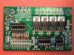
Fig.9 |
| Fig
7. & 8. Showing installation of the MOSFETs.
Fig 9. Fit
the three IC sockets to the PCB. Make sure all the
pins go through the holes in the PCB and check that none
of the pins have bent
under the socket before soldering.
Each socket has an 'D'
shaped indent at one end. This should align with
the marking on the component screen print overlay.
|

Fig.10 |
Fig.11 |
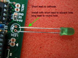
Fig.12 |
| Fig 10.
Fit the 78L05 voltage regulator to the PCB.
The pins may need
realigning to fit the holes in the PCB. Take care
to position it so the flat part of the body is aligned
with the flat shown on the component screen print
overlay.
Fig 11. Fit the
330nF capacitor C1. This is marked .33J63
(alternative part 470nF marked .47K63)
Fig 12. Fit
LED1. One lead is shorter than the other.
This marks the cathode terminal of the LED. Make
sure to install with the short lead in the position
shown in the photo.
|
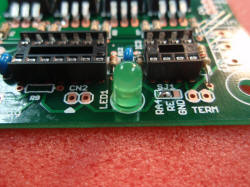
Fig.13 |
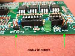
Fig.14 |
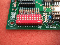
Fig.15 |
| Fig 13.
Showing LED1 installed on the PCB.
Fig 14. Solder the
2-pin header plugs to positions JP1(DMX config) and TERM
as shown in the photo.
Fig 15. Solder
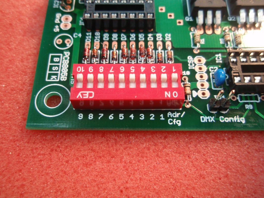
the 10-way DIP switch to the PCB. Make sure to fit
it so the switch 'ON' position is nearest the edge of
the PCB
as shown in the photo. This will make it easier
to follow the configuration examples in the
documentation.
Before soldering the switch into position check that
none of the leads have bent under the switch instead of
going through the PCB hole. This can happen and if
you discover it after you start soldering the switch in
place it's too late.
|
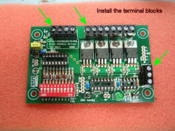
Fig.16 |
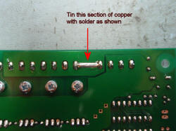
Fig.17 |
|
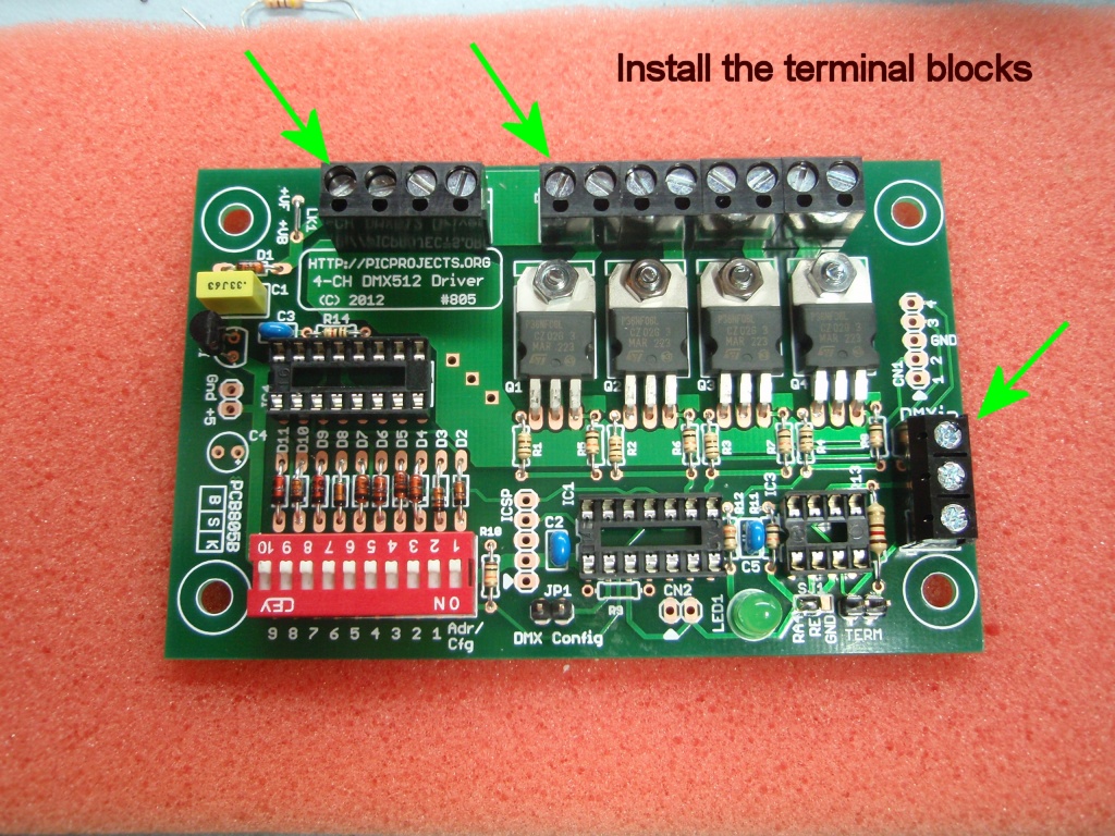
| Fig 16.
Fit the 5mm screw terminal blocks to the PCB.
The DMXin connector
uses a 3-way terminal block.
The other two
connectors use end-stackable 2-way connectors to make up
the 4-way and 8-way blocks. If the supplied
connectors are not already stacked together you should
do this before fitting to the PCB.
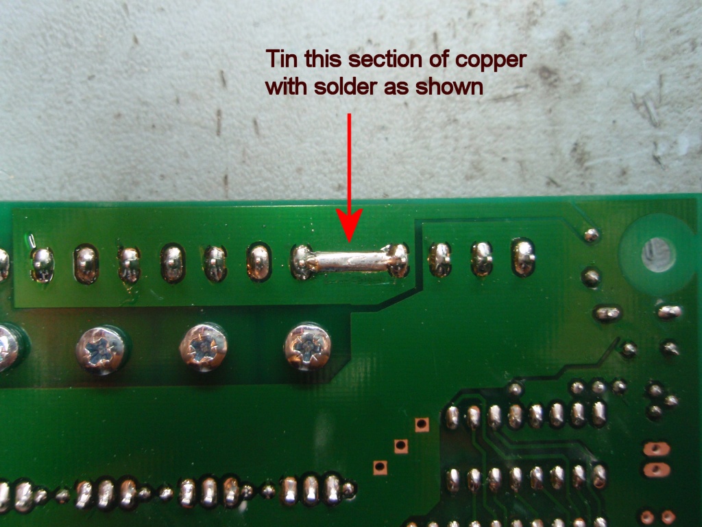
Fig 17. On the
reverse side of the PCB there is a short length of
exposed copper between the terminal blocks. Tin
this section with solder to increase the electrical
current carrying capacity of the PCB track.
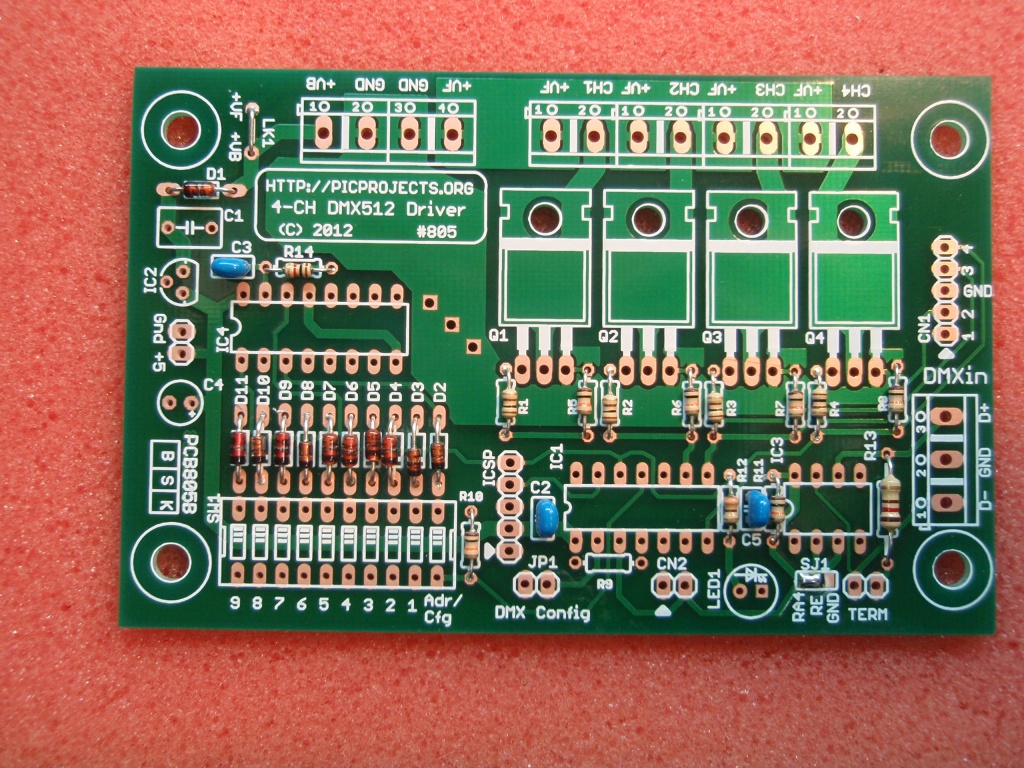
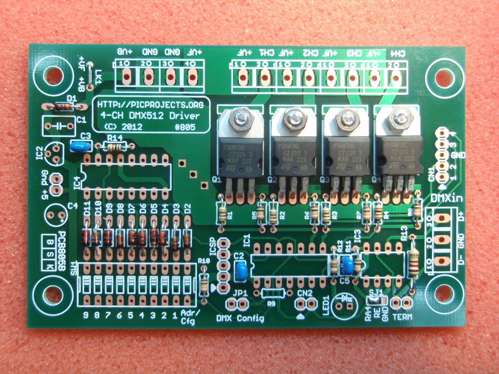
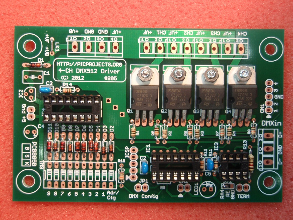
 At this stage the assembly of the board is complete.
Give the board a good visual check to make sure all the
solder joints are good, there are no solder splashes or
bridges on any of the joints. Check components are
in the correct location and orientation where
applicable. At this stage the assembly of the board is complete.
Give the board a good visual check to make sure all the
solder joints are good, there are no solder splashes or
bridges on any of the joints. Check components are
in the correct location and orientation where
applicable.
|
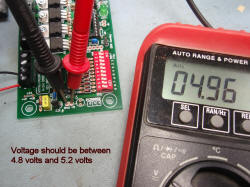
Fig.18 |

Fig.19 |
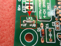
Fig.20 |
|
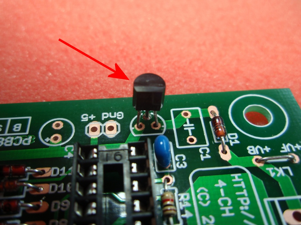
Fig 18.
Before fitting the three IC's into the sockets check the
5 volt power supply to the board.
Connect a suitable DC
power supply to +VB and GND connections of the power
connector terminal block. The power supply output
voltage should be in the range of 9 to 18 volts.
Measure the voltage at
the 5 volt test point on the PCB as shown in the photo.
The voltage measured
here must be between 4.8 volts and 5.2 volts.
If it is not within this range investigate and correct
the fault before proceeding.
Once the 5 volt power
supply has been checked and is working correctly
disconnect the power before proceeding.
Fig 19.
Make sure the board is not connected to the power
supply!
Install
the three ICs into the sockets on the board
- IC1 is a 14-pin
part marked PIC16F1823
- IC3 is a 8-pin
part marked SP485 (alternative part may be
supplied in the kit)
- IC4 is a 16-pin
part marked HCF4017BE
Fit each IC into the
correct socket. Since each IC has a different
number of pins there is only one socket that matches
each device.
Make sure that
each IC is installed with the 'D' shaped indent in the body
matching the indent in the socket. See photo Fig
19.
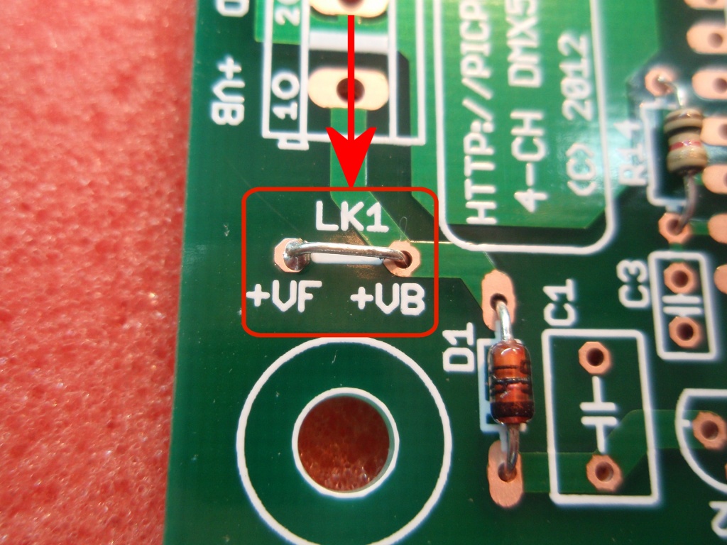
Fig 20. Powering the board.
The control electronics
on the board require a power supply input in the range 9
volts to 18 volts DC. This is made at the +VB and
GND terminals of the 4-way terminal block.
Since the Channel
Outputs can operate between 3 and 36 volts the board may
require separate power sources for the board and channel
power ( +VB and +VF)
If the Channel Outputs
are operating within the 9 volts to 18 volts range
fitting the link wire to position LK1 will connect the
+VF power input to the +VB board supply, eliminating the
need for two power sources or extra wiring at the
connector terminal.
Only fit LK1 if the +VF power supply is within the 9-18
volt range. Below 9 volts the board will not
operate correctly. Above 18 volts components on
the board may be damaged or destroyed.
|
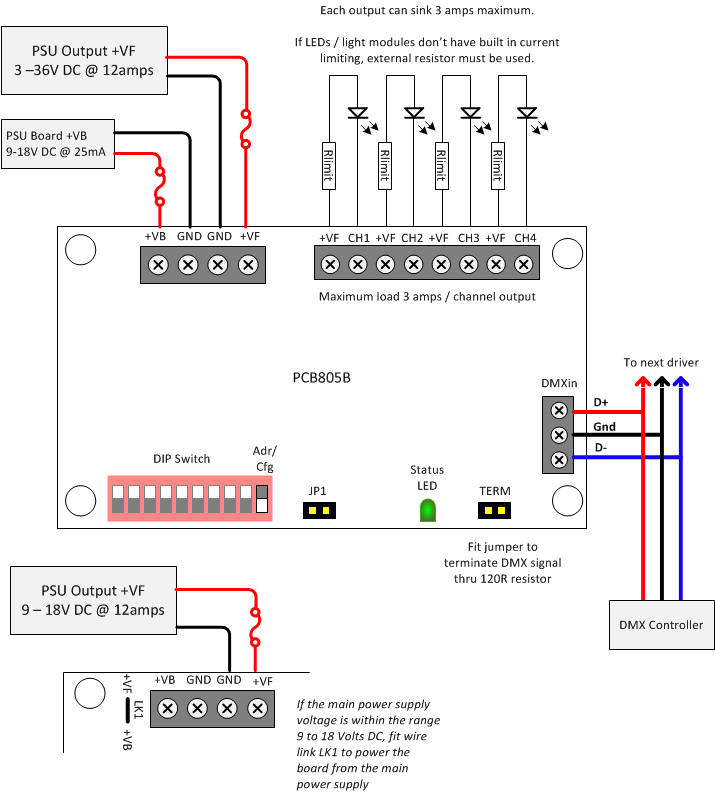
Connecting the board
This is a general
overview of the connections to the 4 Channel DMX512 Driver
PCB805B.
-
When connecting
LED or LED modules to the controller consult the datasheet for
the specific devices being used to ensure voltage and current
limits are met.
-
Do not operate the board at currents or voltages outside the
ranges shown here.
-
Ensure appropriate rated fuses are used in the power supply
connections
-
Ensure correct
wire gauge is used for the current it will be carrying.
-
The +VF
connections shown are all connected to the same common PCB
trace
The GND connections shown are all connected to a common
Ground PCB trace
-
+VF and +VB
are the MOSFET and Board control electronics power inputs
respectively. They are not electrically connected
unless the link wire LK1 is fitted on the PCB. When
fitted LK1 allows the board to derive its power from the +VF
power input. This should only be fitted when the +VF
input voltage is between 9 and 18 volts DC.
|
|
3-pin XLR Wiring for DMX512 |
|
|
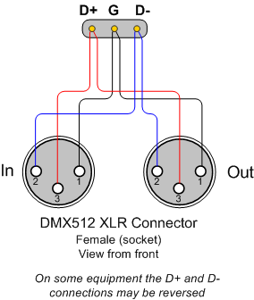
Connection for DMX in-out
using 3 pin XLR socket.
There are also
standards for 5-pin XLR and RJ45 connection.
www.dmx512.com |
Configuring Driver Options
Options Summary
The DMX driver board has
various user configurable options as summarised below.
- Output drive mode
The outputs can be
configured to operate in PWM mode or digital mode. Each channel can be individually configured to operate in
either PWM or digital mode.
In PWM mode the channel output is driven with an 8 bit
resolution PWM signal at 200Hz. The duty cycle is
derived from the DMX channel data with 0 = 0% through to 255 = 100%
In digital mode the channel output is either on or off. The DMX channel data controls the output
- Channel data value 0 - output turns OFF
- Channel data values 1-254 - no change at output.
- Channel data value 255 - output turns ON
- Ganged Mode
When Ganged mode is enabled, all four outputs are controlled
by the DMX data in the base address channel
- No DMX signal received
output behaviour
When the driver stops
receiving valid DMX data the outputs can be configured to
either remain in their current state / maintain the PWM duty
cycle, or turn off / set PWM duty cycle to 0%.
The time from the last valid packet being received to
entering the stopped state is approximately 1.5 seconds.
- DMX channel base address
for the driver
Can be set from 1 to 509
As there are 4 outputs on the board the highest base
address that can set is 509 since the fourth output channel
then sees data at the highest DMX address of 512.
Methods for Configuring the DMX
Driver
The driver can be configured
using the following methods:
- using a DMX controller to send the configuration as
in-band channel data.
- On-board DIP switch sets
both DMX base address and configuration modes
Settings made through the DIP switch are saved to the
microcontroller's internal EEPROM.
Since the DIP switch is dual function it is used to set both
address and configuration depending on the position of the
Adr/Cfg switch. This means only one of the two
parameters can be set at any time. The non-active
parameters are therefore read from the internal EEPROM.
i.e. If the DIP switch is set to configure the DMX base address,
configuration modes are then set using the values saved to
EEPROM.
Setting the DMX Base Address and Configuration using In-band DMX
config
The firmware
pre-programmed into the PIC microcontroller also supports
In-band configuration over the DMX data channel. This allows the
address and configuration mode settings to be set in custom
designs that do not use the DIP Switch.
In order to use this method of
configuration the DMX controller must be capable of allowing the
channel data values to be set precisely. Controllers that
don't display the actual channel data value cannot be used
since it's not possible to tell precisely what value has been
set.
To configure the driver using DMX
channel
data:
- Connect a physical jumper
to JP1.
- Cycle power to the board.
- Channel data is read from
the first valid DMX packet received and used to configure
the driver as shown in the table below.
- Once the options have been
programmed into the EEPROM the driver will blink its status
LED in a repeating 2 blink pattern.
- Remove the physical jumper from JP1
- Cycle the power to the
driver to restart using the new settings.
- Watch the status LED to ensure the assigned DMX address
is valid
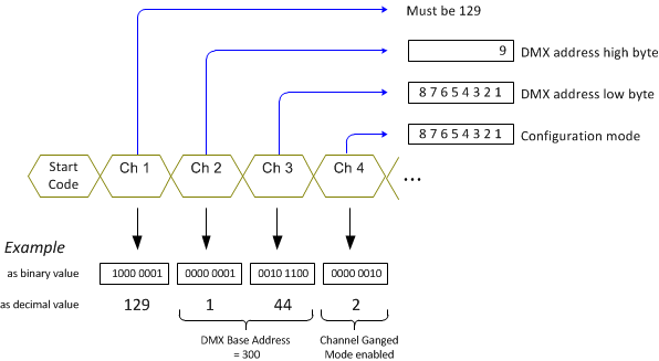
When JP1 is fitted, regardless of the
currently configured DMX base address, the board will read the data
from the first four channels of the DMX data frame.
-
Channel 1 must contain the value
129 for the firmware to accept the frame.
-
Channel 2 contains the 9th
bit of the binary DMX base address
-
Channel 3 contains bits 8 to 1
of the binary DMX base address
-
Channel 4 contains the
configuration mode byte.
After the firmware receives the
complete frame the DMX address and configuration word are saved
to the microcontrollers EEPROM. The firmware does not do any
validation of the data at this time.
When the data has been written to the
EEPROM the status LED1 will blink twice and this repeats continually
until JP1 jumper has been removed and the power cycled.
When the board restarts with JP1
jumper removed, the firmware validates the DMX address. If it is
not in the range 1 to 509 it will signal an error through the
status LED1.
If a DIP switch is fitted, the address or configuration
mode set in-band will be overwritten by the switch setting at
the next power-cycle after JP1 jumper has been removed.
This can be prevented by setting all the DIP switches to the OFF
position which is the same as having no DIP switch installed.
The binary bit positions in the
channel data bytes correspond to the DIP switch
position number shown in the diagram below. To configure
the board with DMX in-band data set the bit positions to '1' or
'0' in the channel data as you would the DIP switch to ON or
OFF.
A ‘0’ in the bit positions
corresponds to the DIP switch number being set to OFF
A ‘1’ in the bit positions
corresponds to the
DIP switch
number being set to ON
Any unused bits should be set to
'0'
DMX Base Address
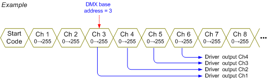
The driver board
receives data over four consecutive channels starting at the
base address configured on the board. The base address can
be set to start at any address in the DMX packet, however it
also needs to be set to an address compatible with the DMX
controller. Some controllers expect the start address to
be located at fixed offsets, eg. 1, 7, 13, 19, 25...
Refer to your controllers documentation.
Setting the DMX Base Address using the
DIP switch
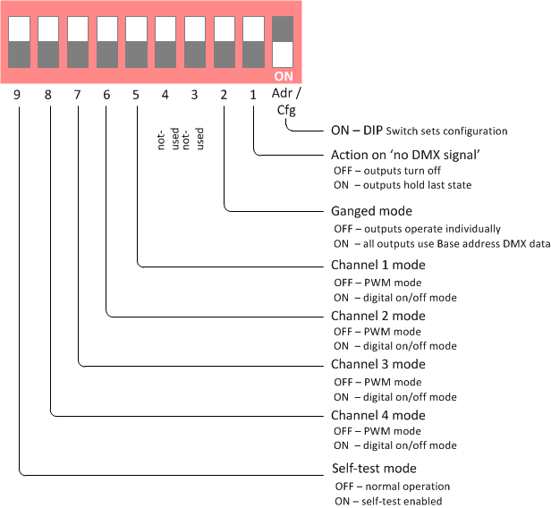
Adr/Cfg switch should be set to
OFF.
The firmware then uses the rest of the DIP switch to set the DMX
base address.
Switches 9 to 1 are
used to set the binary value of the DMX Base Address used by the
board.
Switches set to the
OFF position correspond to a binary value of 0
Switches set to the ON position correspond to a binary value
of 1
The DIP
switch is only read when the board is powered-on. The address
setting read from the switch is automatically saved to the
microcontroller EEPROM. When no DIP switch is present, or the
switch is set to Configuration Modes, the value previously saved
to the EEPROM will be used.
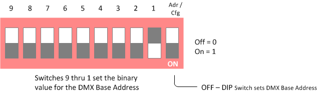
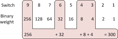
Example: To set the base
address to 300, set switches 9,6,4 & 3 to the on position.
256 + 32 + 8 + 4 = 300
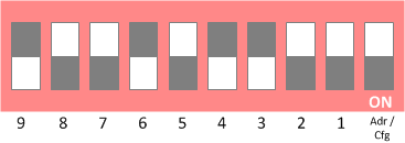
Google will convert decimal to
binary (see example below).

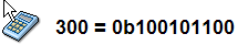
Ignore the leading 0b and set
the switches so 1 = switch ON and 0 = switch OFF
Setting
the Configuration using the DIP switch
Adr/Cfg
switch should be set to ON.
The firmware then uses the
rest of the DIP switch to set the mode configuration for the
driver board.
Action on no DMX
signal received. When no DMX
signal is received the controller can either turn all outputs
off, or continue to drive the outputs with the last PWM or
digital output value for the channel before the DMX data signal
was lost.
Ganged Mode.
In ganged mode all four outputs
use the data from the Base DMX Address.
The table below shows the address used for the channel data
depending on whether the DIP switch is ON or OFF
| |
Channel-1 |
Channel-2
|
Channel-3 |
Channel-4 |
|
Base Address |
ON/OFF
|
ON |
ON |
ON |
|
Base Address+1 |
|
OFF |
|
|
|
Base Address+2 |
|
|
OFF |
|
|
Base Address+3 |
|
|
|
OFF |
Channel Mode.
Each output can operate in either PWM or digital mode. The operating mode can be set for each channel
individually.
In PWM
mode the output is driven with a PWM signal, the duty cycle is set
by the DMX data value:
0 = 0% thru 255 = 100%
In digital mode
the output is either on or off.
-
When the DMX data value is 0 the
output turns off.
-
When the DMX data value is 255 the output
turns on.
-
DMX data between 1 and 254 is ignored and will not
change the output.
Self-Test.
When self-test mode is enabled each output turns on at 0.5
second intervals until all outputs are on (100% PWM duty).
Each output then turns off at 0.5 second intervals until all
outputs are off (0% PWM duty). This repeats continuously until
the self-test DIP switch is set to the OFF position and power is
cycled to the board. During self-test, any data received
on the DMX channel is ignored.
Operation
DMX Channel data
PWM mode
|
Channel |
Value |
Function |
|
|
1 |
0 - 255 |
PWM 0% - 100% |
|
|
2 |
0 - 255 |
PWM 0% - 100% |
|
|
3 |
0 - 255 |
PWM 0% - 100% |
|
|
4 |
0 - 255 |
PWM 0% - 100% |
|
Digital mode
|
Channel |
Value |
Function |
|
|
1 |
0
1-254
255 |
Off
no-change
On |
|
|
2 |
0
1-254
255 |
Off
no-change
On |
|
|
3 |
0
1-254
255 |
Off
no-change
On |
|
|
4 |
0
1-254
255 |
Off
no-change
On |
|
Connectors / Headers /
Jumpers
Board power (+VB / GND)
Input power for the driver
board. 9-18 volts regulated DC @ 25mA
Channel power (+VF / GND)
The MOSFET channel power is
applied to the +VF / GND connector terminals.
Voltage range is 3 to 36 volts DC
Maximum current per channel is 3 amps giving maximum input
power of 12 amps.
The current
rating of the power supply will depend on the devices being
driven. Ensure you use a suitable power supply for
your application.
Note:
If the MOSFET channel power
supply is within the range 9 to 18 volts, fitting the LK1
link wire on the PCB will allow the board to use the +VF
power supply input eliminating the need for two power
sources or extra wiring at the connector terminal.
CH1,CH2,CH3,CH4
Low side switched outputs
connected to the onboard MOSFETS. Channel 1 is
controlled by data sent to the DMX base address of the
board, channels 2,3 and 4 to the next 3 consecutive
addresses.
In Ganged mode all four
channel outputs use data in the DMX Base Address data frame
Do not exceed 3 amps per channel absolute
maximum.
There is no fault
protection on the outputs so depending on your application
you may want to use suitably rated in-line fuses.
DMXin
Connects to the DMX data
cable. Since there are various DMX connector standards
you'll need to wire this to the particular connector you are
using e.g. XLR-3pin, XLR-5pin, RJ45 jack.
TERM
When the jumper is closed,
the DMX signal is terminated into a 120 ohm resistor on the
board. This should only be done on the last board.
Also, if an external cable terminator is used, don't
terminate on the board.
JP1
Open,
normal operation
Closed, enable DMX configuration mode
(see text)
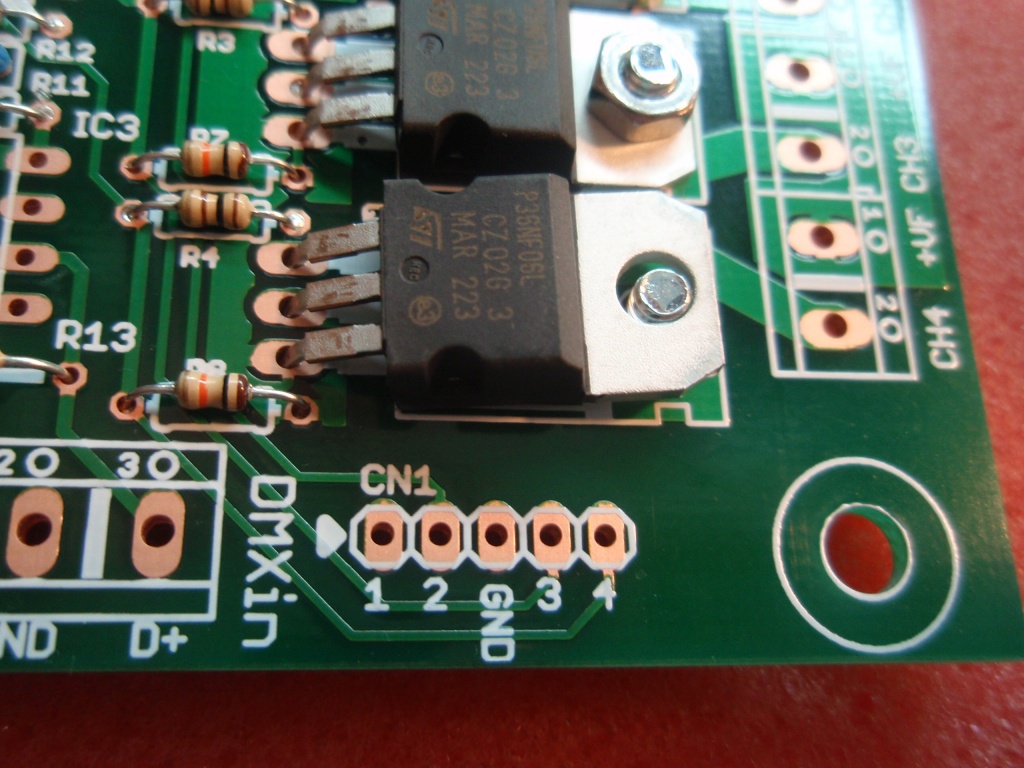
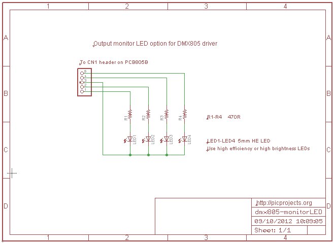
CN1
This 5 pin connector
brings the four channel driver output pins from the
microcontroller to
the edge of the board along with a GND connection.
This makes it easy to interface the driver board to an
alternative output device such as a relay module.
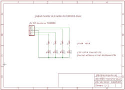 |
CN1
can also be used to connect four output monitor LEDs to
the driver board. The schematic (left) shows
how this can be done if it is required.
Use high efficiency or
high brightness LEDs with current limit resistors no
lower in value than 470R to ensure the MOSFET gate
drive voltage is not adversely affected.
|
ICSP header
This provides a connection
for In-circuit serial programming of the PIC.
Status
LED
The status LED provides
indication that DMX data is being received during normal
operation and error and status codes if a problem is
detected during start-up.
Note: Since the status
LED shares the same PIC control line as a signal on the ICSP
header when the the board is connected to a PIC programmer
the status LED should be ignored until the programmer is
disconnected.
Normal operation
|
LED |
Explanation |
|
On  |
- DMX data received within the last 1.5 seconds
- At power-on
for ~4 seconds (even if no data received)
|
Blinking 0.5Hz
 |
- No DMX data has been received within the last 1.5
seconds
- DMX D+/D-
signal connection reversed.
|
Startup Status Codes
If an error is detected at
power-on the status
LED indicates the detected error condition or status by blinking a number of times followed
by a pause; this repeats continuously. The cause must
be corrected and the driver restarted to clear the condition
and enter normal operation.
| |
LED
blinks |
Cause |
|
2 |
 |
Completed a DMX
in-band
configuration. |
|
3 |
 |
Invalid DMX base
address. =0 |
|
4 |
 |
Invalid DMX base
address. >509 |
|
5 |
 |
EEPROM write failed
after 5 retries |
|
6 |
 |
PIC internal GPR
memory failed to initialise |
- Status code 2 is not
an error. Once the DMX configuration has
completed, remove the mode jumper and cycle power to the
board to use the new settings.
- Status codes 3 and 4
indicate the DMX base address for the board is invalid.
Re-program a valid address, using either the DMX address
board, DMX in-band configuration
- Status codes 5 and 6.
If these can't be cleared by cycling power to the board,
then the PIC is faulty and should be replaced.
Firmware
DMX805 PWM LED Driver
Firmware
DMX
Compatibility
We've tested the DMX driver
board with the following DMX controllers:
DMX512 test data
transmitter.
This small application
generates 8 frames of DMX data in channels 1 to 8. The
data in channels 1 to 4 increments from 0 to 255 in a repeating
pattern. Data in channels 5 to 8 is always zero.
This code was written to allow
testing of the DMX Driver with a DMX data stream where the
Break, MAB, packet idle time, packet length, etc could all be
configured. This was required since many commercial
products don't generate DMX packets with minimum timing
parameters and it was necessary to ensure the application code
would work reliably under these conditions.
This code has been provided to
allow testing of the DMX Driver described on this web page with
a consistent DMX512 data packet stream. The DMX output
from this code generates a Break of 94uS, MAB of 5.8uS and an
idle time between packets of 5uS. Channel data is sent
back-to-back with no delay.
|
Description |
Filename |
Download link |
DMX transmitter test code
HEX file
ready to program into a PIC16F688 |
dmx688demotx.HEX
V1.0.0 15/10/2012
|
 download
checksum 7347 |
Example schematic for testing
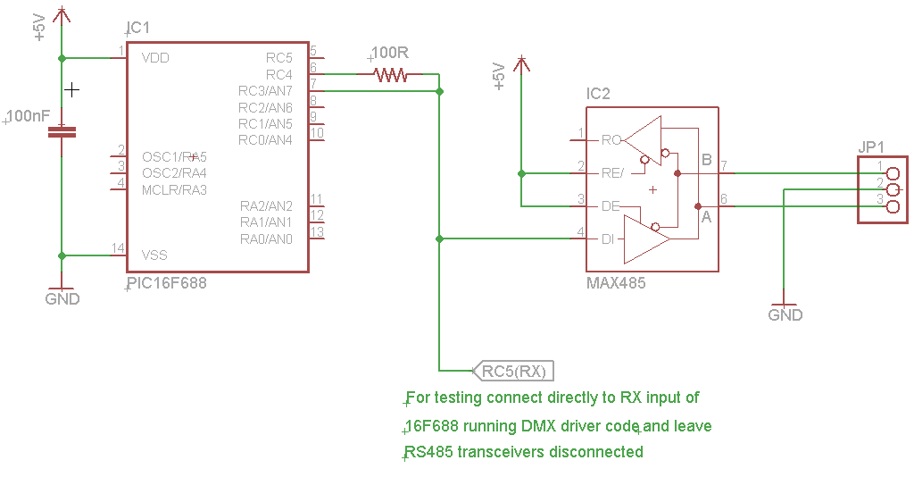
|