|
PWM
DC Motor
Controller
for PIC12F683
|
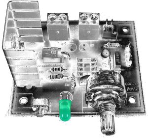 |
Description
There are lots of designs on
the Internet for DC power controllers using Pulse Width
Modulation (PWM) to control the speed of a motor or power to a
resistive load. Most
of these use analogue methods to generate the PWM signal which in
turn drives a power MOSFET or transistor.
When I wanted a speed controller for the PCB drill I use to make
all my PIC Projects what else could I do but design a PWM Power
Controller around a PIC - a practical PIC project for sure.
I came up with a fairly
straightforward design based on a
PIC12F683 using the
Capture/Compare/PWM
(CCP)
peripheral inside the PIC to generate a PWM output. An 'N'
Channel Logic Level MOSFET in a low side configuration is driven
by the PIC to control the output power to the motor.
A variable resistor provides a
voltage input to the PIC which is converted to a digital value
using the onboard Analogue to Digital convertor, this in turn is
used to set the PWM duty cycle. Since the PWM duty cycle
is adjusted using a voltage signal input to the PIC it is
possible to use an alternative analogue front-end instead of VR1
to provide this voltage input and therefore control of the duty
cycle.
|
In the original version of
this project the input from the Analogue to Digital
Converter (ADC) was fed directly to the duty cycle
register of the PWM module on the PIC, therefore the PWM
output duty changed linearly in direct proportion to the
change in input voltage to the ADC; much the same as an
analogue PWM. The switch
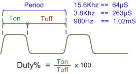
input allowed the PWM period to be selected in one of
three ranges; 15.6Khz, 3.8Khz and 980Hz.
The significant feature in
the new version of the firmware which sets it apart
from analogue PWM is that it now uses the input from the ADC as an index to a
data table. This table contains the required output duty cycle
and period. By creating a suitable table of data
you can map any value at the input of the ADC to any duty
cycle and one of 3 fixed periods at the PWM output.
The switch input now
cycles through 3 mapping tables. The default
tables supplied with the code have a one-to-one mapping
of input voltage to duty cycle output and fixed periods
of 15.6Khz, 3.8Khz and 980Hz respectively to keep it
backward compatible with the original version of the
code.
More details of this and
example map table files can be found in the
Operation section.
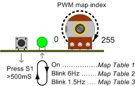
A push button cycles through
three different mapping tables. The mapping table in use is saved to EEPROM so it always
powers up using the last selected table; an LED indicates
the current setting.
There is also a digital control
input that allows the output driver to be turned off. When
pulled low the PWM output is set to 0%.
|
Example of log10 map
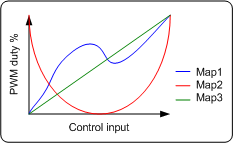
Example of three map
tables, each with
completely different remap data |
|
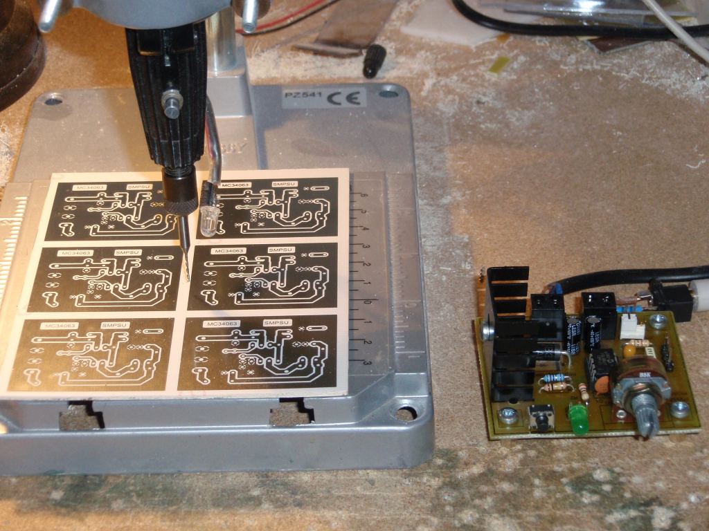
connected to PCB drill |
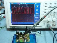
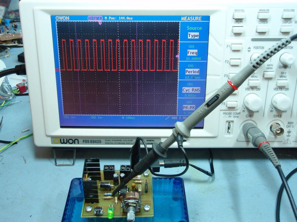
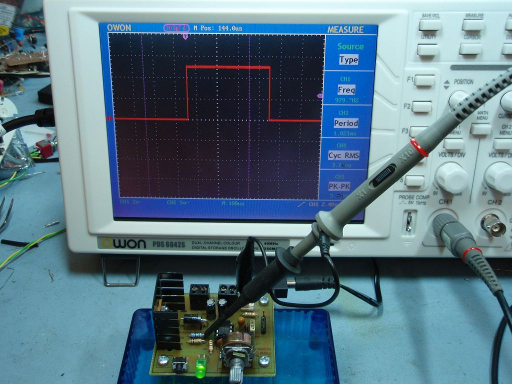
Showing
PWM signal on oscilloscope |
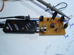
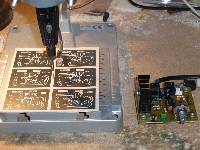
Code development prototype |
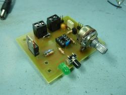
Prototype PCB |
Schematic
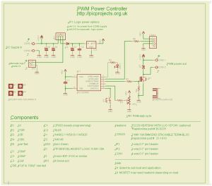
Download
schematic in PDF

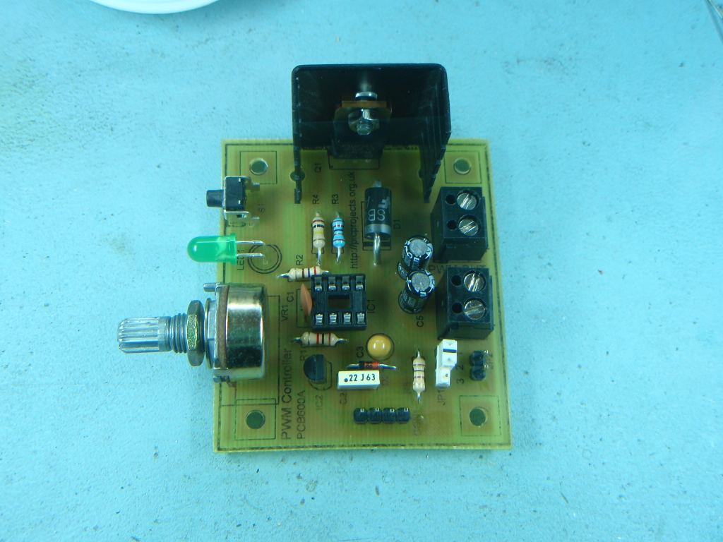
Circuit Description
The PIC12F683, IC1 has an
internal hardware PWM peripheral that is used to generate the
PWM signal. The duty cycle of the PWM signal is controlled by
VR1 which via R1 presents a voltage on pin 3 of IC1.
With 0V on the input the duty cycle is 0% (off) up to 100% with
5 volts at the input. The PWM signal is output
from pin 5 of IC1 and drives the gate terminal of Q1 through R3.
Resistor R4 connects the gate terminal of Q1 to ground. This ensures that Q1 remains off when the circuit is first
powered on as the I/O pins of IC1 are all set to inputs until
the firmware initialises them as outputs. Diode D1 is
required when driving inductive loads and provides a path for
the inductive flyback current. For loads up to 3 amps Q1
does not require a heatsink, above this you may need to use one.
Power for the logic is provided
by IC2, a 78L05 5 volt regulator. It connects to the input
voltage source via diode D2 which provides protection against
reverse polarity connection of the supply. The 3-way
jumper JP1 allows the input voltage for the 78L05 to be taken from
either the main power
input or an auxiliary supply. When a jumper is connected between pins 1 and 2
power comes from the main DC input.
Since the maximum input voltage for a 78L05 is 30 volts there
may be applications where a separate power supply is needed for
the logic. This is catered for by connecting a jumper between
pins 2 and 3 of JP1 and connecting an alternate power supply to
JP2.
Switch SW1 allows one of three
PWM remap tables to be selected. To avoid accidental
changes to the map table in use the firmware requires the switch
to be held for at least 500mS before switching to the next map
data table. The table selected is indicated by LED1 and the
value is saved to EEPROM so it always powers up using the last
used setting.
CON1 provides a digital input which
is polled by the firmware. When this input goes low the
duty cycle is set to 0% from the start of the next PWM period,
this turns MOSFET Q1 off.
When the input returns high the PWM restarts using the duty
cycle set by the input from VR1. The connector also provides 5v and Gnd connections to allow
connection of a small off-PCB control circuit. If it
is used to power another circuit, ensure it doesn't draw more than
40mA from the supply. If the shutdown control isn't
required, leave the connector open and the PICs internal
weak-pull-up will hold the input high enabling the PWM output.
The circuit as shown will work
with input voltages from 9 to 20 volts. If you choose to
use it with a higher input voltage you may need to select
different components (see notes below)
Notes:
- Since the power controller
can work with a DC input voltage from 9 volts up to 40 volts
or higher the following components need to be suitably rated
for the specific application the controller will be used
for:
- Q1 and D1 need both
voltage and current ratings to suit the application.
- C2,C3,C5,C6 should
have a voltage rating greater than the input voltage.
- IC2 needs minimum of
8.5 volts and absolute maximum of 30 volts.
- Q1 is a logic level MOSFET and
is designed to be driven by a low gate voltage. Standard MOSFETs
will generally work as a substitue in low power applications.
- For the flyback diode D1 a 1N4002 can be used here for
most low power applications, a 1N5819 Schottky is better, for
higher current loads a 1N5820, SB330 or SB350 might be preferred.
- To get the full range of control when VR1 is rotated
fully CCW, check that the voltage on the wiper terminal of
the VR1 is at 0 volts. The voltage on the VR1 wiper
terminal must go from Vss to Vdd to get the full output range.
- Potentiometer VR1 is specified as 5K on the schematic but it can be
substituted with a 4K7 part or a 10K. In all cases it needs
to be a linear (LIN) type not logarithmic (LOG).
- The PIC MCLRE reset input (pin 4 ) is set to input with
the reset logic internally tied to Vdd and a weak-pull up
enabled on the I/O pin.
Limitations
This is a very basic PWM power
controller and it does have some limitations. These are
not design flaws, but the result of the design goal for the
project which was low cost and simplicity. Therefore please note the
following:
- There is no current limit
or overload sensing, you may need to use a fuse inline with
the load.
- The PWM controller is open
loop so it does not adjust the duty cycle to maintain a
constant motor RPM as the load changes. You could add
an analogue PID control loop at the ADC input to achieve
this if it is required.
- The design with components
specified will work at supply voltages up to 20 volts and output
loads around 3 amps, possibly higher depending on whether
the load is inductive or resistive. With
alternate components the circuit could be used with load
voltages and current greater than this. However it
should be noted that since the MOSFET is driven directly by
the output from the PIC, there is a limit as to the
voltage/current and type of loads that can be switched
before it becomes necessary to use a dedicated MOSFET gate
driver between the PIC and the MOSFET.
Photos above show the PWM
output at the three operating frequencies.
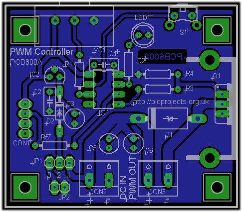
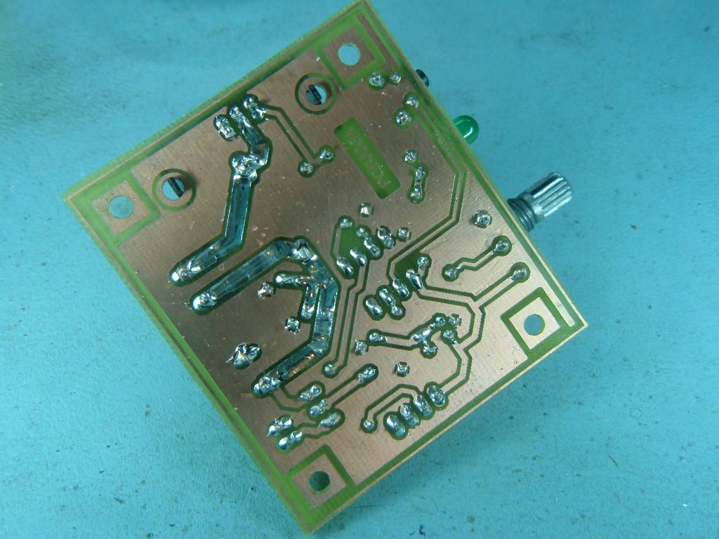
PCB Layout
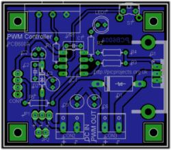
Download PCB
artwork in PDF
Download Eagle 5.3.0 CAD Files (ZIP)
Component List
You can buy all the parts
needed to build this project from most component suppliers world
wide. In the UK you can get everything from Rapid Online and
I've included a parts list with their part numbers below.

All
Rapid parts/descriptions correct at 16-November-2008. You should
check part# and descriptions are correct when ordering in case
I've made a mistake transferring them onto this page.
Ordering parts from
Rapid?
Use the cut & paste quick order form on their
home page
with this list of
parts

Components in this list are
suitable for use with an input voltage in the range 9-22
volts DC
| Component |
Description |
Part # |
| R1 (order 1
pack) |
PACK 100 1K 0.25W CF
RESISTOR (RC) |
62-0370
|
| R2 (order 1
pack) |
PK 100 270R 0.25W CF
RESISTOR (RC) |
62-0356 |
| R3 (order 1
pack) |
PACK 100 220R 0.25W CF
RESISTOR (RC) |
62-0354
|
| R4 (order 1
pack) |
PK 100 100K 0.25W CF
RESISTOR (RC) |
62-0418
|
| R5 (order 1
pack) |
PK 100 100R 0.25W CF
RESISTOR (RC) |
62-0346
|
| VR1 |
16MM 4K7 LIN.
COMMERCIAL POT. (RC) |
65-0710
|
| C1 |
100N 5MM PITCH CERAMIC
DISC CAPACITOR RC |
08-0235 |
| C2 |
220NF 63V 5MM
POLYESTER BOX CAPACITOR RC |
10-3264 |
| C3 |
22UF 25V TANTALUM BEAD
2.5MM RC |
11-1050 |
| C5, C6 |
47UF 25V LOW IMPEDANCE
ELECTROLYT CAP RC |
11-2921 |
| |
|
|
| D1* |
1N5819 SCHOTTKY DIODE
DO-41 RC |
47-5322
|
| D2 |
1N4148 SIGNAL DIODE
75V 150MA (TRU) RC |
47-3416
|
| Q1 |
STP36NF06L MOSFET
LOGIC N 60V 30A (RC) |
47-0552
|
| IC2 |
DA78L05 V REG +5V
100MA TO-92 TRU (RC) |
47-3612 |
| LED1 |
L-7113GD LED 5MM GREEN
DIFF 20MCD (RC) |
55-0120
|
| socket for IC1 |
8 PIN 0.3IN TURNED PIN
SOCKET(RC) |
22-1720 |
| IC1** |
PIC12F683-I/P
MICROCONTROLLER (RC) |
73-3374
|
| CON1, JP1,
JP2 (order 1)*** |
10W SINGLE
ROW PCB HEADER PLUG RC |
22-0515 |
| CON2, CON3 |
2 WAY 16A
5MM END STACKABLE TERM-BLOC RC |
21-1810 |
| Heatsink
(if needed) |
TO220
HEATSINK WITH LUG 19°C/W (RC) |
36-0235 |
| S1 |
3.85MM
RIGHT ANGLE TACT SWITCH (RC) |
78-1152 |
| Jumper
(use with JP1) |
OPEN BLUE
2.54MM JUMPER LINK (RC) |
22-3555 |
Parts List Notes
*
D1 may need to be
changed for a higher rated part if used with inductive loads at
high currents.
** IC1 will need
programming with the firmware code
before use
*** Order a single 10way
header for CON1, JP1, JP2 and then cut into lengths of
4-way, 3-way and 2-way
There is no capacitor C4,
the component labels jump from C3 to C5
PIC Programmer
If you need a PIC programmer you can also buy the PICkit2 starter kit from Rapid, part #
97-0101
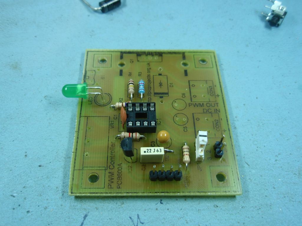
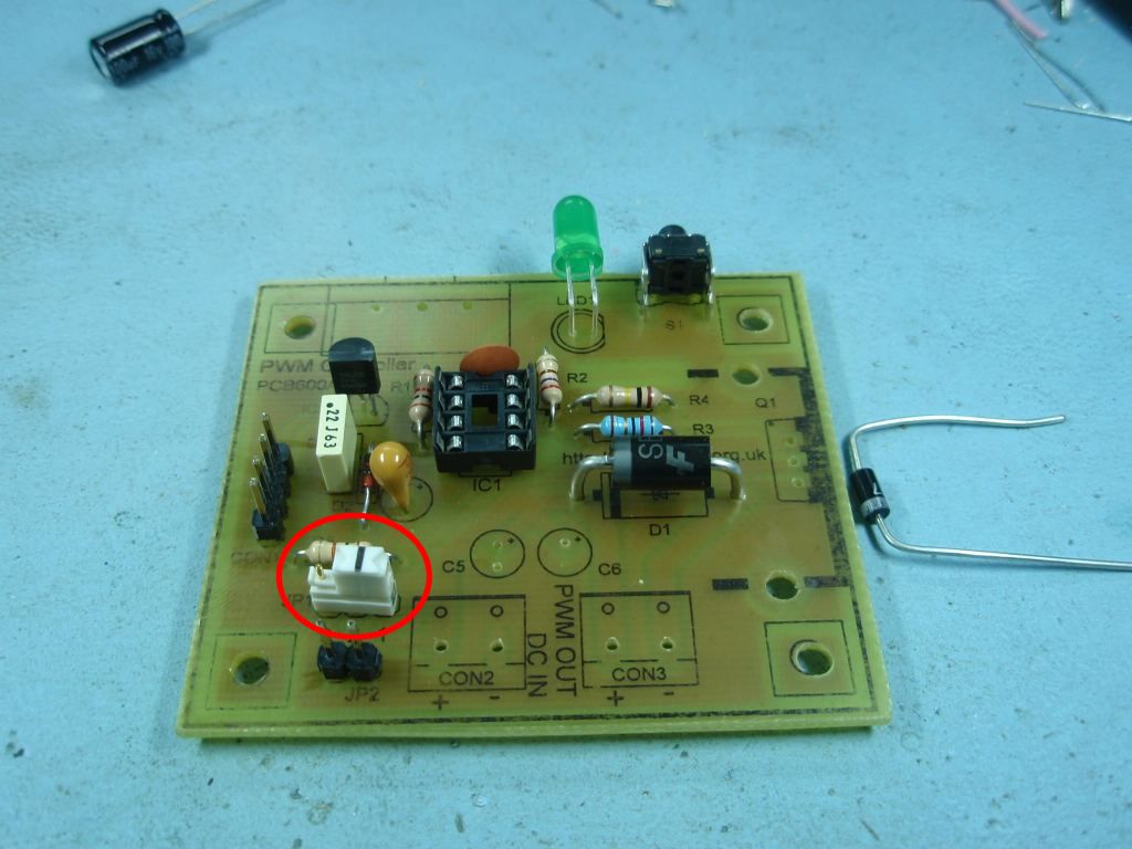
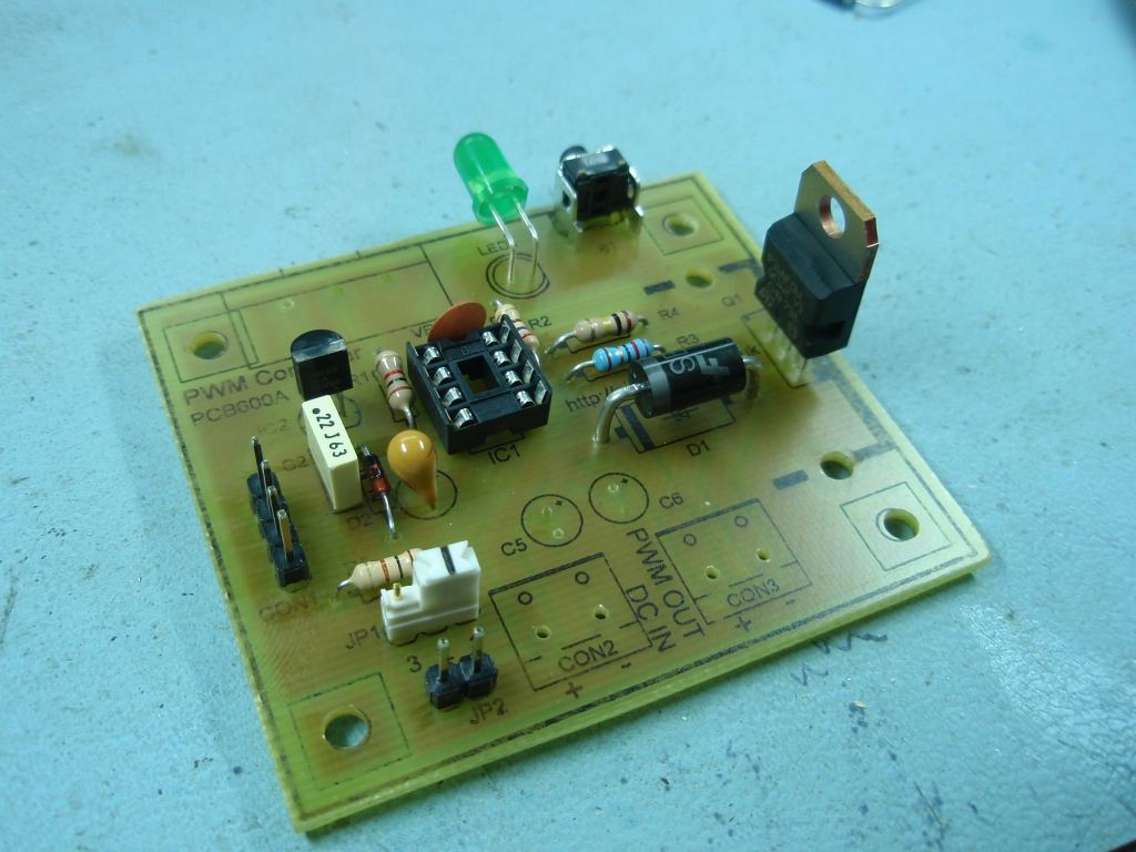
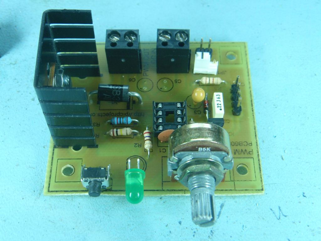
Construction photos:
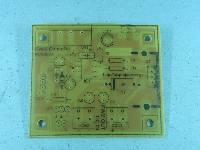
Fig.1
|
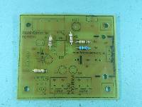
Fig .2 |
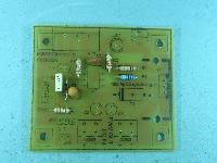
Fig. 3 |

Fig.4
|
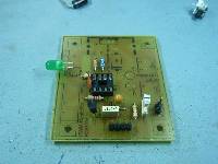
Fig .5 |
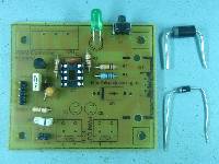
Fig. 6 |
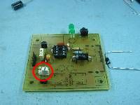
Fig.7
|

Fig .8 |
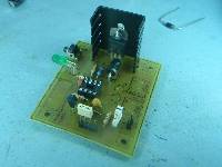
Fig. 9 |
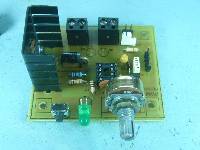
Fig.10 |
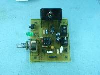
Fig .11 |
Fig. 12 |
Fig 1. Start assembly
with the small components first and work through to the large
parts. Be careful to observe anti-static handling
procedures when installing the MOSFET Q1, to avoid destroying
it.
Fig. 4 The LED has its
legs bent through 90o before installation
Fig.6
Diode D1 depends on the type and power rating of the load.
The PCB will take a large body diode but you can also use the
smaller 1 amp types as your application requires.
Fig.7
Install shorting jumper across pins 1+2 of JP1 as shown.
If you know exactly what how you will be using the controller, a
cheaper option is to simply install a wire link instead of JP1.
Fig.8/9
With loads up to 3 amps Q1 doesn't need a heatsink. Above
3 amps it will need one and even if the load is under 3 amps it
won't hurt to fit one anyway.
You do not need to use an
insulating washer kit between the heatsink and the MOSFET since
the heatsink is isolated on the PCB. However, since the
heatsink is connected to the MOSFET you need to make sure it
doesn't come into contact with any other parts of the circuit or
any enclosure you install the controller into.
Fig.12
Heavily tin with solder the PCB tracks between the
connectors and MOSFET to increase the current carrying capacity
of these tracks. This is shown in the photo.
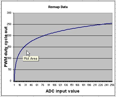
Operation
Controls
In use, VR1 controls the duty
cycle (and period) of the PWM output. The analogue input
from VR1 is used as an
index to the map table which returns the required PWM duty cycle
and period. This means a linear input at the ADC can
be used to generate a non-linear change in duty cycle at the
output.
An example of where this can be
useful is controlling the brightness of an LED. The
apparent brightness of an LED does not respond in a linear
fashion to increases in duty cycle. By creating a suitable
remap table, a linear change at the ADC input can be remapped to
a duty cycle curve that produces an apparent linear increase in
brightness of the LED.
Another significant feature of
using the ADC input as an index to a lookup table is that not
only does it allow the duty cycle to be remapped but the PWM
period can also vary in response to the input at the ADC.
Taking advantage of the
available memory in the PIC MCU, three remap tables can be
programmed into the PIC. Switch input S1 is used to select the map table to be
used .
Pressing S1 for > 500mS will cycle through three map tables; this is to avoid accidental
operation. The table in use is indicated by the LED as
shown below. The map table selected for use is also
saved to EEPROM so when the PIC is next powered on it will use
that last selected table.
The default map tables supplied
with the code use a linear mapping of input voltage to output
PWM duty cycle. Each table has a fixed PWM period.
| Map Table 1,
PWM period 15.6KHz
Map Table 2, PWM period 3.8KHz
Map Table 3, PWM period
980Hz
Example include files:
|
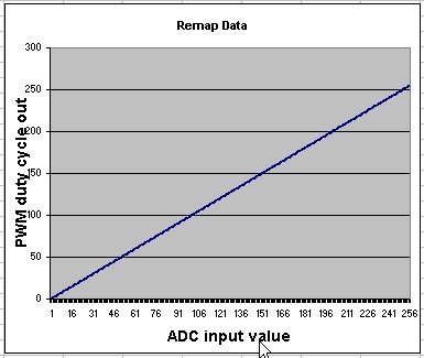
Linear input to output
duty cycle map |
Alternate Map Tables
The map data used
by the firmware can be changed by editing the
bdcm_remap.asm file and entering alternate include
file names for the required map tables. The
section to edit can be found at the end of the
file (example below). The semicolon comments
the line out, removing it will cause the line to be
included during assembly. There should always
be three remap data files included. These can
be different files or the same one included three
times.
;
---------------------------------------------
; Include up to 3 remap data include files here
;
; ---------------------------------------------
; 1st include -> remapSelect 0 -> LED on
#include
remapData1.inc
; 2nd include -> remapSelect 1 -> LED 6.2Hz
#include
remapData2.inc
; 3rd include -> remapSelect 2 -> LED 1.5Hz
#include
remapData3.inc
;#include remapData4.inc
;#include remapData5_log10.inc
New tables can be
created using a spreadsheet. Copy and past the required
cells into MPLAB and save as someMapFile.inc.
Include the names of the map files in the bdcm_remap.asm
file and reassemble.
Example spreadsheet
table (Excel 2003)
The duty cycle value used in
the map table should be a integer in the range 0 to 255.
To convert the duty cycle as a percentage to a value for the map
table, multiply by 2.55
e.g. 60% x 2.55 = 153
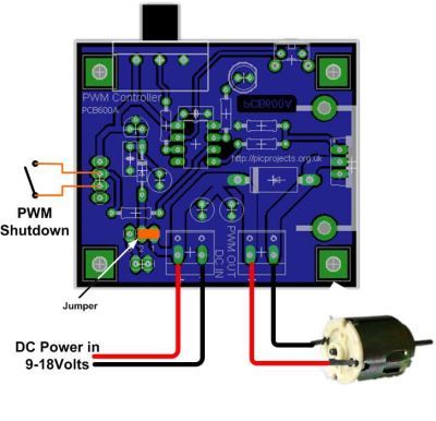
Connecting the PCB
Connect DC input power to CON2
and the output load to CON3. The PWM Shutdown input is
optional, if it's not required leave the connector disconnected
and the output will be enabled.
Safety
Warning:
The shutdown control input should not be used as
an emergency stop. |
Firmware
The HEX file is ready to
program directly into a PIC 12F683. The asm file contains the
source code which you can modify or just view to see how it
works. If you are going to modify the code I recommend you
download and install the
Microchip MPLAB IDE which will allow you to edit, modify and
program the PIC seamlessly.
If you need a PIC Programmer I
strongly recommend the
Microchip PICKit 2,
this is available from suppliers world wide or direct from
Microchip.
Not got a programmer? Buy
a pre-programmed PIC from the On-line store
|
Description
|
Filename
|
Download link
|
|
Source code for 12F683
|
bdcm_remap108.zip
v1.0.8 22/07/2018
|
download
|
|
HEX file ready to program into
the PIC
Standard version
|
bdcm_remap108_standard.HEX
v1.0.8 22/07/2018
|
download
|
|
HEX file ready to program into
the PIC
Soft Start enabled version
|
bdcm_remap108_SoftStart.HEX
v1.0.8 22/07/2018
|
download
|
Version
1.0.3 - Fixes a code bug which caused the two least significant bits of the
PWM
duty cycle value to be reversed.
Version
1.0.4 - Soft Start version
Version
1.0.5 - Fixed issue with duty cycle update causing noise at low settings
Added assembly time option to change internal Fosc
frequency which allows
different PWM periods/frequency to be used.
Set clock to 1Mhz for PWM frequency of (3.9Khz, 950Hz, 245Hz)
Set clock to 2Mhz for PWM frequency of (7.8Khz, 1.9Khz, 490Hz)
Set clock to 4Mhz for PWM frequency of (15.6Khz, 3.8Khz, 980Hz)
Set clock to 8Mhz for PWM frequency of (31.2Khz, 7.6Khz, 1.96Khz)
Added 8 byte rolling average filter to ADC input signal
Made common code base so there are no longer separate versions for standard
and Soft Start code. Options can be selected in the bdcm_remap_10x_common.asm
file prior to assembly.
Version
1.0.6 - Force 100% PWM output when duty value = 255. Because of
the way the PWM
peripheral hardware works within the PIC itself, setting the duty cycle register
to
255 actually only gets to 99.6% duty. This update forces it to 100% (always
on)
so it behaves as you would
expect.
Version 1.0.7 - Clear
PWM CCPR1L and DC1B1/DC1B0 bits of CCP1CON before enabling
PWM module since the value in the register is undefined after reset which can
cause a one cycle random output of the PWM at power-on.
Fixed
issue where changing the selected map would not register until the ADC duty
cycle input value changed. Now when a
new map is selected it forces an update of the PWM registers with the new map
values.
Version 1.0.8 - Fix
issue where PWM output doesn't restart after the RunStop input has been
activated until the input from the duty cycle potentiometer has changed
Soft start version
The Soft Start code features a soft
start at power up. If you imagine having the control
potentiometer set at zero and rotating it to its final position
each time the controller is powered on this is a soft start.
Instead of doing this manually, the control potentiometer can be
left in any position and the output is automatically 'ramped' up
to the current position of the control potentiometer each time
the controller is powered on.
If the control potentiometer is
at maximum it takes approximately 1.2 seconds for the output to
ramp up to the final setting, the time taken is directly
proportional to the position of the control position; for
example if the control is at 1/3 maximum it takes 1.2/3 = 0.4
seconds.
This code version is identical
to the original in respect to the operation of the modes and
lookup data tables for the remap functionality described
elsewhere on this project page.
This code will not work
with the PIC 12F629 or PIC12F675 since they do not
have the required internal CCP peripheral used to generate the
PWM signal.
|