|
|
Radio Button
Switch Control
with switching overlap / deadband delay
for PIC12F629
|
 |
Overview
The original purpose behind this
circuit was to provide manual switching of three relays such that
only one relay was on at any time. It was also a requirement
that there was a specific overlap (or make-before-break) period.
The code was then further developed to provide deadband
(break-before-make) as well as overlap switching. The mode and
timing delay are stored as parameters in the PICs EEPROM memory
making editing of these straightforward without the need to
reassemble the source code.
This circuit controls up to three
outputs using a 'radio button' type switching control. When
any one of the channel inputs is selected, the corresponding output
is turned on and all other outputs are turned off.
If you're not familar with 'radio' buttons they work like this:
In addition to this the controller
features adjustable deadband or overlap of the outputs during
switchover.
- With dead band delay or
break-before-make operation the active output is turned off
before the new output is turned on.
- With overlap or
make-before-break operation the new output is turned on before
the active output is turned off.
The delay is configurable in
0.512mS intervals from 0 to 130.56mS
The control inputs also feature a
configurable debounce timer with the same range of timings making it
suitable for use with simple switches directly attached to the PIC
or logic interface.
Although designed to control relays
the firmware is quite generic and can be used in any application
where 'radio button' functionailty is needed.
(14/11/2012 -
Source code and firmware
for 8 Channel version for PIC16F628A)
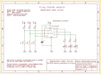
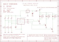
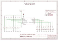
Schematic
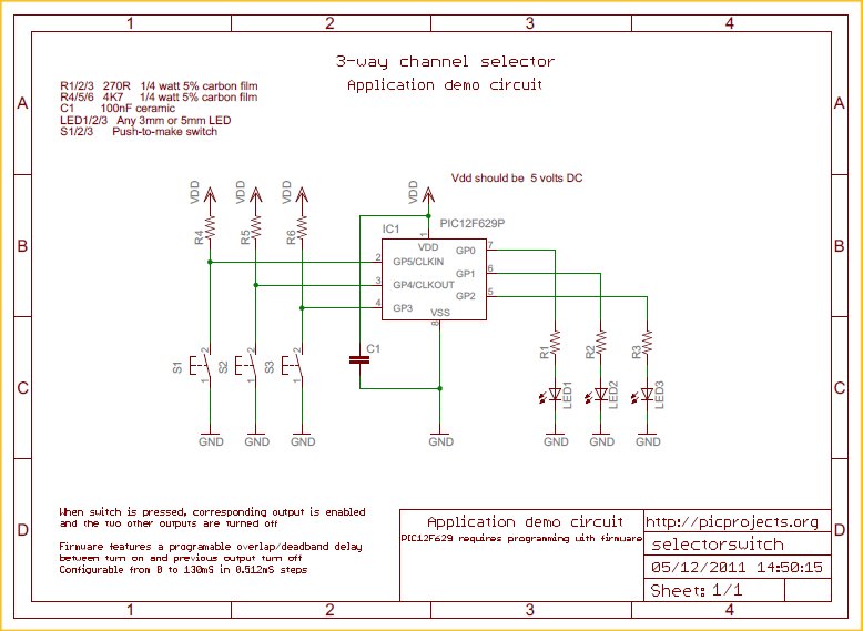
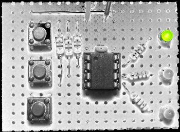
| 3 Channel evaluation
circuit
 |
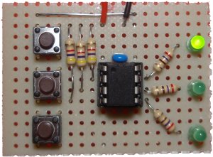
Evaluation circuit from schematic #1
built on prototype board
|
schematic #1
 |
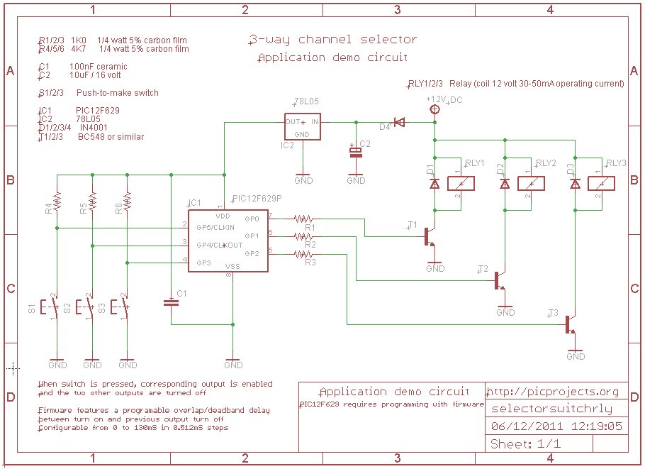
| 3 Channel Relay Control
 |
|
schematic #2
|
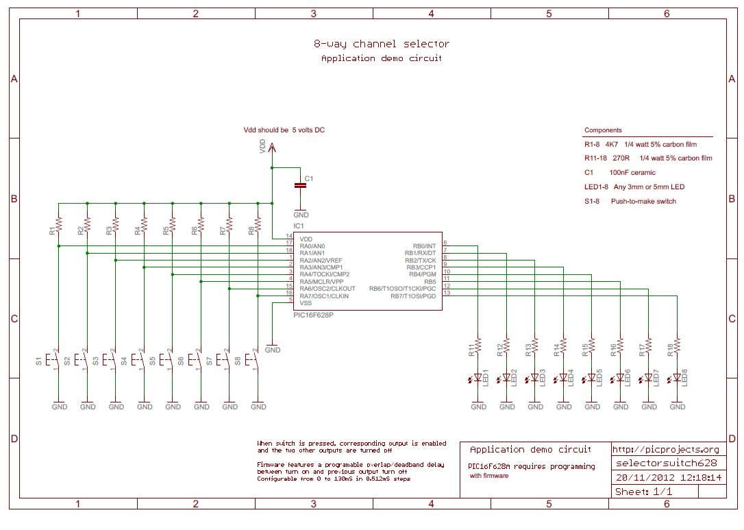
| 8 Channel evaluation
circuit
 |
|
schematic #3
|
The schematics above are intended
to show the general application of the Radio Button Switch Control.
Schematic #1 and #3 in particular can be used to build a simple firmware
evaluation circuit.
Mode
Examples
In this section I've used a
Saleae Logic
tool to illustrate the output operating modes and effect of input
switch debounce delay.
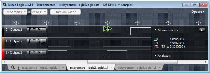
Make-before-break
In the example below Output 3 turns on
before Output 2 turns off. The overlap is 99.36mS as the T1-T2
marker flags show
made with a
Saleae USB 8 channel logic analyzer for mac, PC or linux
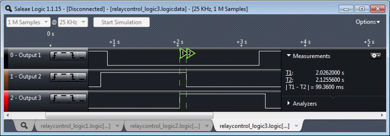
Break-before-make
In the example below Output 2 turns off
before Output 3 turns on. The deadband is 124mS as the T1-T2
marker flags show
made with a
Saleae USB 8 channel logic analyzer for mac, PC or linux
No-delay output switching.
In the example below there is no delay.
Output 2 turns off at the same time as Output 3 turns on. Within
the code new output values are written to the PICs GPIO port by a single
instruction.
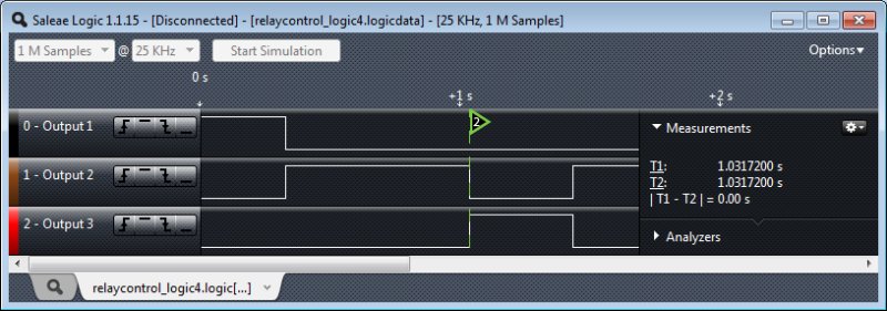
made with a
Saleae USB 8 channel logic analyzer for mac, PC or linux
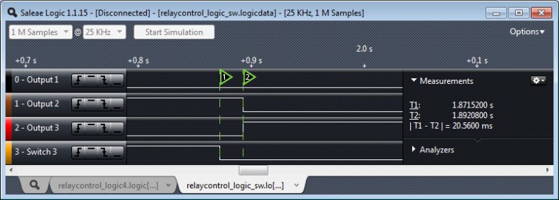
Control input switch debounce
In the example below you can see the
debounce delay on the switch input. T1 marker flag shows the point
where the Switch 3 button is pressed, the input goes low. At the
T2 marker flag, 20.56mS later outputs 2 and 3 change state (the firmware
is configured for zero delay so the outputs change simultaneously)
made with a
Saleae USB 8 channel logic analyzer for mac, PC or linux
Firmware notes:
-
All timings are
derived from the PICs internal RC oscillator and accuracy is
dependant on the same.
-
The main code is
interrupt driven so all switching events are
synchronous with the interrupt
interval of 512uS (0.512mS)
-
The switch inputs are
only sampled at each interrupt so even with the switch debounce
timer set to zero there may be a delay of up of up to 512uS before a
output switching event occurs.
-
Within the interrupt
handler there are additional delays depending on the mode and switch
debounce timing. These are not specified but fall in the range of
10-30 microseconds and are deterministic.
Since the firmware code was originally written to operate mechanical
relays under the control of manual push button switches this timing
accuracy was considered sufficient and is likely to be so for any
similar application.
However, you should take this into account when considering it for
use in a specific application.
Configuration
-
 Firmware
is configured from data held in the PICs EEPROM. The data
values are entered in hexadecimal. Firmware
is configured from data held in the PICs EEPROM. The data
values are entered in hexadecimal.
-
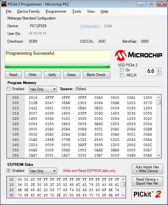
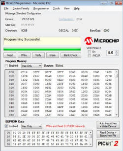
Using the
PICkit2 standalone programmer application first load the HEX
file into the application (see firmware
section).
-
Next edit the
three values in the EEPROM Data window to suit the
requirements of your particular application.
-
Use the
programmer to write the Program Memory and EEPROM data to
the PIC12F629
-
Put the
programmed PIC into the application circuit and test.
|
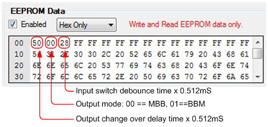
-
EEPROM Address 0x00
Make/Break delay time interval in 0.512mS steps.
Range from 00 to FF (0 to 255 decimal)
HEX code download set to FF (255) = 0.512mS x 255 = 130mS
-
EEPROM Address 0x01
Output mode:
00 -> Make-Before-Break MBB
01 -> Break-Before-Make BBM
HEX code download set to 00 (0) = MBB mode
-
EEPROM Address 0x02
Input switch debounce timer interval in 0.512mS steps.
Range from 00 to FF (0 to 255 decimal)
HEX code download set to 28 (40) = 0.512mS x 40 = 20.48mS
To convert decimal
values to hexadecimal you can use Google. Ignore the '0x' part
of the answer and use the two alpha-numerics. e.g. 0xA0
enter A0 in the EEPROM data.

Firmware
You will need a PICkit2/3
programmer and the free software that comes with the programmer.
The latest versions of MPLAB and PICkit2 standalone application can
be downloaded from the Microchip
website
3 Channel version for PIC12F629
|
Description |
Filename |
Download link |
|
Source code for 12F629 |
ctrlswitch.asm,
v1.0.0, 05/12/2011 |
 download
 |
|
HEX
file ready to program into the PIC
|
ctrlswitch.HEX, v1.0.0, 05/12/2011
|
download
checksum 0x0CB9 |
8 Channel version for
PIC16F628A
|
Description |
Filename |
Download link |
|
Source code for 16F628A |
ctrlswitch628A.asm,
v1.628B, 18/11/2012 |
download |
|
HEX
file ready to program into the PIC
|
ctrlswitch628A.HEX, v1.628B, 18/11/2012 |
download
checksum 0xBA09 |
Contact us:
 |